Micro Molding Creates Micron-Sized Features with High Precision
Micro Molding Creates Micron-Sized Features with High Precision


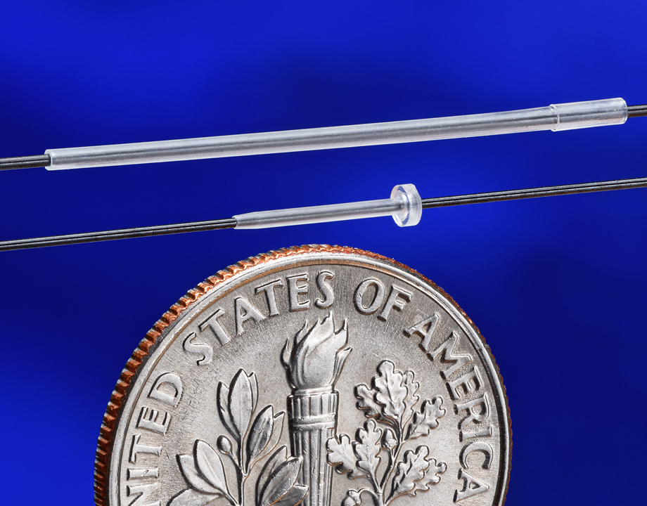
Precise, thin walls are possible with micro injection molding. Two examples are a drug delivery straw (top) with 0.005-inch walls, and a cannula (bottom) with 0.0025-inch walls.
Engineers are always trying to pack more functionality into the same available space or less, which calls for smaller components, thinner walls, and more creative geometry. Much of this can be achieved with micro molding.
This manufacturing process produces extremely small, high-precision components with micron tolerances. In expert hands, micro molding can produce features under one micron in size and walls as thin as 25 microns. This expertise is especially in demand for the medical device, electronics, and analytical instrumentation fields.
The increasing complexity of these products often pushes molding technology to new limits. As a result, molders are using all their talents and specialized materials to achieve complex designs for their clients, often turning around production-ready or prototype-ready micro-molded components in as little as two days.
One approach that can expand the capabilities and speed of micro molding is combining it with other technologies in complementary ways, such as using additive manufacturing (AM) to build detailed, pre-production molds.
In the past, engineers were required to cut hard steel to make tooling for early-stage designs. Now, engineers can produce molds and prototypes faster and at lower cost using AM methods, such as digital light processing (DLP), saving significant processing time.
“There is steady advancement in new or improved materials that can be micro-molded with high precision,” said Kenny Freitag, sales manager for specialty molding and medical tubing for Spectrum Plastics Group. “For example, polyether ether ketone, or PEEK, can be formulated with different fillers that enhance mechanical performance.”
Continue the Topic: Using Micro 3D Printing for Short-Run Production
Micro-molding PEEK, however, requires a solid understanding of its melt characteristics, such as flow path, and temperature must be carefully monitored. “Miniaturization also creates challenges with understanding material flow and shear, for example,” he added. “Using highly engineered materials that enhance functionality also gives engineers a wider range of design options.”
Many new micro-medical applications utilize bioabsorbable materials so that implantable devices made from these materials dissolve into the body after a certain amount of time. This eliminates the need for additional surgery to remove a device, which elevates the risk of infection or other adverse effects. These sensitive materials must be handled carefully and stored in temperature-controlled environments to avoid degradation. Specialized or customized micro-molding equipment is required to control processing factors like residence time, shear, and degradation rate of material during molding.
“This limit can change drastically given the complexity of the part geometry, application of the device, and the type of polymer material,” said Kyle Kolb, tooling supervisor for MTD Micro Molding. “Different materials respond differently to factors such as pressure loss, compressibility, and even thermal conductivity, which can influence how quickly a flow front cools and how drastically the viscosity increases as flow continues.”
Become a Member: How to Join ASME
How small a feature can be depends on the type of feature and the mechanical and physical properties of the selected material. For example, lower-viscosity resins tend to fill thinner features better because they flow more easily and evenly, achieving wall thicknesses as small as 0.0015 inches.
As demand grows for components with miniaturized dimensions, “we also need to be thinking about how to measure these parts after molding,” said Maggie Beauregard, quality manager for MTD Micro Molding. “Non-contact vision systems or computerized tomography [CT] scanners allow hands-off inspection, which minimizes damage from handling.”
CT scanning provides high accuracy and repeatability at the sub-micron level, saving days of measurement time. For example, if a product’s quality check requires that 50 dimensions be measured, it typically takes three to four days using standard metrology; it only requires a single day with CT. Additionally, CT scanning can show the inside of a component to identify flaws that do not appear on the surface.
As micro molders continue to go smaller, there will eventually be a dimension that is unachievable—a point at which the design collides with the material itself.
“In one project, the customer had to switch to a mineral-filled resin because the original glass filler was getting in the way—the micro shards of glass were too big for the part we were producing,” said Aaron Johnson, vice president of marketing and customer strategy for Accumold.
You Might Also Enjoy: Metal Injection Molding or Metal Additive Manufacturing: Which One is Best for Your Project?
Parts will continue to become smaller and more complex, challenging the limits of molding technologies. Materials will be developed that are for specific micro molding processes and that have greater functionality and can hold tighter tolerances.
“Ultimately, the Internet of Things will allow the integration of sensor technologies, machine-to-machine communication, artificial intelligence, and cloud-based platforms to become integrated into micro-molding systems, maximizing production quality and efficiency, and reducing operational costs and downtime,” said Freitag.
Mark Crawford is a technology writer based in Corrales, N.M.
This manufacturing process produces extremely small, high-precision components with micron tolerances. In expert hands, micro molding can produce features under one micron in size and walls as thin as 25 microns. This expertise is especially in demand for the medical device, electronics, and analytical instrumentation fields.
The increasing complexity of these products often pushes molding technology to new limits. As a result, molders are using all their talents and specialized materials to achieve complex designs for their clients, often turning around production-ready or prototype-ready micro-molded components in as little as two days.
One approach that can expand the capabilities and speed of micro molding is combining it with other technologies in complementary ways, such as using additive manufacturing (AM) to build detailed, pre-production molds.
In the past, engineers were required to cut hard steel to make tooling for early-stage designs. Now, engineers can produce molds and prototypes faster and at lower cost using AM methods, such as digital light processing (DLP), saving significant processing time.
Material Choices
A wide range of materials is available for micro molding, including plastics, metal, and ceramics. Continual improvements in engineered materials can provide very specific chemical and physical properties.“There is steady advancement in new or improved materials that can be micro-molded with high precision,” said Kenny Freitag, sales manager for specialty molding and medical tubing for Spectrum Plastics Group. “For example, polyether ether ketone, or PEEK, can be formulated with different fillers that enhance mechanical performance.”
Continue the Topic: Using Micro 3D Printing for Short-Run Production
Micro-molding PEEK, however, requires a solid understanding of its melt characteristics, such as flow path, and temperature must be carefully monitored. “Miniaturization also creates challenges with understanding material flow and shear, for example,” he added. “Using highly engineered materials that enhance functionality also gives engineers a wider range of design options.”
Many new micro-medical applications utilize bioabsorbable materials so that implantable devices made from these materials dissolve into the body after a certain amount of time. This eliminates the need for additional surgery to remove a device, which elevates the risk of infection or other adverse effects. These sensitive materials must be handled carefully and stored in temperature-controlled environments to avoid degradation. Specialized or customized micro-molding equipment is required to control processing factors like residence time, shear, and degradation rate of material during molding.
Shrinking Limits
“How small can you go?” is often the first question that micro molders hear from clients regarding a new product idea or design. As hopeful as clients are for their designs, there is a practical limit to size that is driven by the molder’s ability to control material degradation, induce manageable stresses, and incite flow into a mold cavity with repeatability.“This limit can change drastically given the complexity of the part geometry, application of the device, and the type of polymer material,” said Kyle Kolb, tooling supervisor for MTD Micro Molding. “Different materials respond differently to factors such as pressure loss, compressibility, and even thermal conductivity, which can influence how quickly a flow front cools and how drastically the viscosity increases as flow continues.”
Become a Member: How to Join ASME
How small a feature can be depends on the type of feature and the mechanical and physical properties of the selected material. For example, lower-viscosity resins tend to fill thinner features better because they flow more easily and evenly, achieving wall thicknesses as small as 0.0015 inches.
As demand grows for components with miniaturized dimensions, “we also need to be thinking about how to measure these parts after molding,” said Maggie Beauregard, quality manager for MTD Micro Molding. “Non-contact vision systems or computerized tomography [CT] scanners allow hands-off inspection, which minimizes damage from handling.”
CT scanning provides high accuracy and repeatability at the sub-micron level, saving days of measurement time. For example, if a product’s quality check requires that 50 dimensions be measured, it typically takes three to four days using standard metrology; it only requires a single day with CT. Additionally, CT scanning can show the inside of a component to identify flaws that do not appear on the surface.
As micro molders continue to go smaller, there will eventually be a dimension that is unachievable—a point at which the design collides with the material itself.
“In one project, the customer had to switch to a mineral-filled resin because the original glass filler was getting in the way—the micro shards of glass were too big for the part we were producing,” said Aaron Johnson, vice president of marketing and customer strategy for Accumold.
You Might Also Enjoy: Metal Injection Molding or Metal Additive Manufacturing: Which One is Best for Your Project?
Parts will continue to become smaller and more complex, challenging the limits of molding technologies. Materials will be developed that are for specific micro molding processes and that have greater functionality and can hold tighter tolerances.
“Ultimately, the Internet of Things will allow the integration of sensor technologies, machine-to-machine communication, artificial intelligence, and cloud-based platforms to become integrated into micro-molding systems, maximizing production quality and efficiency, and reducing operational costs and downtime,” said Freitag.
Mark Crawford is a technology writer based in Corrales, N.M.


