Evolving Optical Metamaterials through Optimization Algorithms
Evolving Optical Metamaterials through Optimization Algorithms
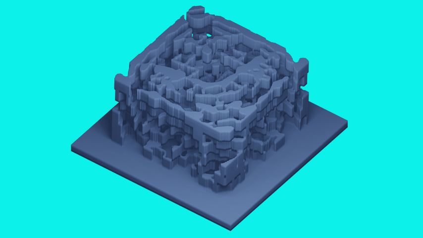
Researchers at California Institute of Technology have pioneered a new technology to design optical metamaterials in three dimensions.
Materials scientists, physicists, and engineers have long looked to optimize optic metamaterials, nanometer-sized structures designed to support specific optical properties by manipulating the behavior of light in novel ways, to enhance cameras, sensors, and visual displays. For the most part existing meta-materials have, to date, worked in two dimensions. Now, researchers at the California Institute of Technology (CalTech) have developed a new method to evolve and optimize optic metamaterials in three dimensions, allowing designers to explore new degrees of freedom at a high spatial resolution.
Andrei Faraon, William J. Valentine Professor of Applied Physics and Electrical Engineering at CalTech, said he has long been interested in what might be possible with 3D meta-optics and what capabilities they may allow for new applications.
“With objects that are structured in three dimensions at a sub-wavelength scale, you can achieve various optical transformations hard to do via other means,” Faraon explained. “Often, you have an optical set-up that is comprised of multiple lenses on an optical table and then some filters that can send different wavelengths of light to the different parts of the set-up. Maybe you want red light to go in one direction, blue light in another. To do this, you need to utilize multiple components. But if you can structure things at a sub-wavelength scale in a 3D optic metamaterial, you can create a single object that does multiple functions at the same time.”
To create such objects, Faraon and graduate student Gregory Roberts leveraged an optimization algorithm and two-photo polymerization (TPP) lithography, a precise 3D printing method that uses a laser to harden liquid resin and easily allows for structures with nano-scale features. When asked about the greatest challenges in coming up with this pioneering new approach to designing optic metamaterials, Faraon said the optimization algorithm is “computationally intensive.”
“Generally, we like to work in 2D or quasi-2D components. But when you are working in three dimensions, the number of degrees of freedom and the number of variables involved are very large,” he said. “It becomes complicated to store your entire structure on a computer and then simulate it so you can evolve the electromagnetic fields you want in that structure.”
That said, the optimization algorithm allows the designers to input specifications for particular optical behaviors and then iterates the design of the structure until it meets those criteria. The resulting nano-sized structures are unique, with a “chaotic” appearance. Faraon said that given they are trying to create functions that may split wavelengths in a specific pattern, it makes sense that the resulting structures have such a singular appearance. The research team then tested structure designs using simulation tools before printing.
“The tricky part is choosing the correct parameters,” he said. “Once you test the design, if you want to fabricate something, you need to have sufficient spatial resolution to get the target function. It’s very important, as you test your design, that you have a sense of where you want to be in terms of the resolution and the size of the object so you can get specs that are close to what you need.”
While Faraon and team have developed this new design and fabrication method as a proof of concept, he is confident that, with more research, these unique 3D optic metamaterials could be made with a practical manufacturing technique. But first, he cautioned, it is important to define the application you are creating the structure for and see whether it makes sense from a cost/benefit perspective.
“These processes are expensive and you need to identify the applications where it’s worth the resources to make these structures,” he said. “There is a relatively clear path toward making a manufacturable practical device, but it would need to be for a targeted application. Like if you wanted to make a compact instrument with very specific optical properties for a space application, it is probably worth investing in this kind of nanofabrication.”
While it may take time to realize the most useful applications for this technique, Faraon believes that 3D optic metamaterials are an “untapped frontier” well worth exploring.
“In the near future, I think we will see applications, first in the longer wavelength range of medium infrared and the long wave infrared, where you can actually reliably make these kinds of structures with photography techniques,” he said. “Soon, I think we will see these types of devices in specialized defense and space applications and, as the technology matures, we will probably see these structures in consumer electronics and in imaging devices. It’s just going to take some time.”
Kayt Sukel is a technology writer in Houston.
Andrei Faraon, William J. Valentine Professor of Applied Physics and Electrical Engineering at CalTech, said he has long been interested in what might be possible with 3D meta-optics and what capabilities they may allow for new applications.
“With objects that are structured in three dimensions at a sub-wavelength scale, you can achieve various optical transformations hard to do via other means,” Faraon explained. “Often, you have an optical set-up that is comprised of multiple lenses on an optical table and then some filters that can send different wavelengths of light to the different parts of the set-up. Maybe you want red light to go in one direction, blue light in another. To do this, you need to utilize multiple components. But if you can structure things at a sub-wavelength scale in a 3D optic metamaterial, you can create a single object that does multiple functions at the same time.”
Optimization algorithm
To create such objects, Faraon and graduate student Gregory Roberts leveraged an optimization algorithm and two-photo polymerization (TPP) lithography, a precise 3D printing method that uses a laser to harden liquid resin and easily allows for structures with nano-scale features. When asked about the greatest challenges in coming up with this pioneering new approach to designing optic metamaterials, Faraon said the optimization algorithm is “computationally intensive.”
“Generally, we like to work in 2D or quasi-2D components. But when you are working in three dimensions, the number of degrees of freedom and the number of variables involved are very large,” he said. “It becomes complicated to store your entire structure on a computer and then simulate it so you can evolve the electromagnetic fields you want in that structure.”
That said, the optimization algorithm allows the designers to input specifications for particular optical behaviors and then iterates the design of the structure until it meets those criteria. The resulting nano-sized structures are unique, with a “chaotic” appearance. Faraon said that given they are trying to create functions that may split wavelengths in a specific pattern, it makes sense that the resulting structures have such a singular appearance. The research team then tested structure designs using simulation tools before printing.
“The tricky part is choosing the correct parameters,” he said. “Once you test the design, if you want to fabricate something, you need to have sufficient spatial resolution to get the target function. It’s very important, as you test your design, that you have a sense of where you want to be in terms of the resolution and the size of the object so you can get specs that are close to what you need.”
Identify application
While Faraon and team have developed this new design and fabrication method as a proof of concept, he is confident that, with more research, these unique 3D optic metamaterials could be made with a practical manufacturing technique. But first, he cautioned, it is important to define the application you are creating the structure for and see whether it makes sense from a cost/benefit perspective.
“These processes are expensive and you need to identify the applications where it’s worth the resources to make these structures,” he said. “There is a relatively clear path toward making a manufacturable practical device, but it would need to be for a targeted application. Like if you wanted to make a compact instrument with very specific optical properties for a space application, it is probably worth investing in this kind of nanofabrication.”
While it may take time to realize the most useful applications for this technique, Faraon believes that 3D optic metamaterials are an “untapped frontier” well worth exploring.
“In the near future, I think we will see applications, first in the longer wavelength range of medium infrared and the long wave infrared, where you can actually reliably make these kinds of structures with photography techniques,” he said. “Soon, I think we will see these types of devices in specialized defense and space applications and, as the technology matures, we will probably see these structures in consumer electronics and in imaging devices. It’s just going to take some time.”
Kayt Sukel is a technology writer in Houston.
Researchers at California Institute of Technology have pioneered a new technology to design optical metamaterials in three dimensions.

Freelance writer, author, and ghostwriter
Related Content

Feb 19, 2026
Surface Roughness Accelerates Hydrogen Embrittlement

A team at Chiba University has identified the causal relationship between the roughness of pipe surfaces and the development of hydrogen embrittlement.

Feb 17, 2026
Mining Seaweed for Minerals

The new frontier of extracting critical minerals from kelp.

Jan 22, 2026
The Secrets in Shark Skeletal Architecture

Merk Lab at Florida Atlantic University is exploring whether the secret for sharks' evolutionary success might lie in their skeletal system.

Jan 13, 2026
Caltech's Autonomous IndyCar
Caltech’s autonomous race car takes on the challenge at Laguna Seca, pushing AI-driven speed and strategy to the limits.