New On-Chip Photonics System Could Reduce Data-Center Costs
New On-Chip Photonics System Could Reduce Data-Center Costs


Researchers have developed an energy-efficient, on-chip method that compensates for the temperature variations that degrade photonic chips--saving energy during data center and supercomputer use.
The U.S. Department of Energy reports that “data centers are one of the most energy-intensive building types, consuming 10 to 50 times the energy per floor space of a typical commercial office building. Collectively, these spaces account for approximately 2% of the total U.S. electricity use.”
Furthermore, as businesses and the public utilize more technology, creating vast new amounts of data for storage and analysis, data centers must keep up with innovation by increasing efficiency and finding ways to reduce operational costs.
One way to do this is compensating for the temperature variations that degrade the silicon photonic chips used in data centers and supercomputers. Significant energy is required to keep these temperatures stable and to maintain performance, which drives up energy costs.
Become a Member: How to Join ASME
Currently, the photonics industry relies on components known as “thermal heaters” to fine-tune the working wavelengths of high-speed, electro-optic devices and optimize their performance. These thermal heaters consume several milliwatts of electricity per device. “That might not sound like much considering that a typical LED lightbulb uses 6 to 10 watts,” said Alan Wang, an electrical engineering professor at Baylor University. “However, multiply those several milliwatts by millions of devices and they add up quickly, so that approach faces challenges as systems scale up and become bigger and more powerful.”
To make these computer applications more efficient, a research team at Oregon State University (OSU) led by electrical engineering professor John Conley (OSU) and Wang has developed a new ultra-energy-efficient method that compensates for these temperature variations that consume energy and degrade silicon photonic chips, leading to earlier replacement.
The circuitry in photonic chips relies on photons to transmit data. Moving at the speed of light, photons enable the extremely rapid, energy-efficient transmission of data. Silicon photonics serves as a useful platform for high-bandwidth, low-energy optical interconnects in data centers and high-performance computer systems.
Combining their expertise in photonic materials and devices and atomic layer deposition and electronic devices, Conley and Wang were able to make working prototypes that controlled temperature variations by controlling gate voltage, requiring very little electric current during operation. This discovery makes it possible to reduce the energy needed for temperature control in these devices by a factor of more than 1 million.
More for You: Podcast: Improving Energy Efficiency in Buildings
This is a big breakthrough for electronic systems. Until now, the photonics industry exclusively relied on thermal heaters to fine-tune the working wavelengths of high-speed, electro-optic devices and optimize their performance. Most thermal heaters consume several milliwatts of electricity per device.
Key to the functional prototypes that Conley and Wang designed are silicon micro-ring resonators (Si-MRRs), which play essential roles in on-chip wavelength division multiplexing (WDM) systems. This is due to their ultracompact size and low energy consumption. However, the resonant wavelength of Si-MRRs is very sensitive to temperature fluctuations and fabrication process variation. “Typically, each Si-MRR in the WDM system requires precise wavelength control by free carrier injection using thermal heaters that consume high power,” Conley said.
The on-chip WDM filters were composed of four cascaded tunable Si-MRRs with metal-oxide semiconductor gates formed by a high-mobility transparent conductive oxide (titanium-doped indium oxide), which show much larger electro-optic efficiencies compared to reversed p-n junctions (boundary or interface between two types of semiconductor materials). Controlling temperature via gate voltage consumed virtually no electric current during the process, saving energy and extending the life of silicon chips.
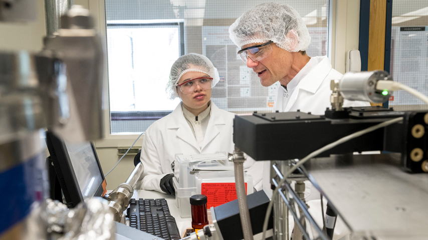
Conley has developed a silicon photonics method that reduces the amount of energy consumed by photonic chips used in data centers and supercomputers. He believes this breakthrough could support the high-speed communication backbone of future data centers and supercomputers. “Our method is much more acceptable for the planet,” he said. “It will one day allow data centers to keep getting faster and more powerful while using less energy so that we can access ever more powerful applications driven by machine learning, such as ChatGPT, without feeling guilty.”
Mark Crawford is a technology writer in Corrales, N.M.
Furthermore, as businesses and the public utilize more technology, creating vast new amounts of data for storage and analysis, data centers must keep up with innovation by increasing efficiency and finding ways to reduce operational costs.
One way to do this is compensating for the temperature variations that degrade the silicon photonic chips used in data centers and supercomputers. Significant energy is required to keep these temperatures stable and to maintain performance, which drives up energy costs.
Become a Member: How to Join ASME
Currently, the photonics industry relies on components known as “thermal heaters” to fine-tune the working wavelengths of high-speed, electro-optic devices and optimize their performance. These thermal heaters consume several milliwatts of electricity per device. “That might not sound like much considering that a typical LED lightbulb uses 6 to 10 watts,” said Alan Wang, an electrical engineering professor at Baylor University. “However, multiply those several milliwatts by millions of devices and they add up quickly, so that approach faces challenges as systems scale up and become bigger and more powerful.”
To make these computer applications more efficient, a research team at Oregon State University (OSU) led by electrical engineering professor John Conley (OSU) and Wang has developed a new ultra-energy-efficient method that compensates for these temperature variations that consume energy and degrade silicon photonic chips, leading to earlier replacement.
Counteracting thermal heaters
The circuitry in photonic chips relies on photons to transmit data. Moving at the speed of light, photons enable the extremely rapid, energy-efficient transmission of data. Silicon photonics serves as a useful platform for high-bandwidth, low-energy optical interconnects in data centers and high-performance computer systems.
Combining their expertise in photonic materials and devices and atomic layer deposition and electronic devices, Conley and Wang were able to make working prototypes that controlled temperature variations by controlling gate voltage, requiring very little electric current during operation. This discovery makes it possible to reduce the energy needed for temperature control in these devices by a factor of more than 1 million.
More for You: Podcast: Improving Energy Efficiency in Buildings
This is a big breakthrough for electronic systems. Until now, the photonics industry exclusively relied on thermal heaters to fine-tune the working wavelengths of high-speed, electro-optic devices and optimize their performance. Most thermal heaters consume several milliwatts of electricity per device.
Key to the functional prototypes that Conley and Wang designed are silicon micro-ring resonators (Si-MRRs), which play essential roles in on-chip wavelength division multiplexing (WDM) systems. This is due to their ultracompact size and low energy consumption. However, the resonant wavelength of Si-MRRs is very sensitive to temperature fluctuations and fabrication process variation. “Typically, each Si-MRR in the WDM system requires precise wavelength control by free carrier injection using thermal heaters that consume high power,” Conley said.
The on-chip WDM filters were composed of four cascaded tunable Si-MRRs with metal-oxide semiconductor gates formed by a high-mobility transparent conductive oxide (titanium-doped indium oxide), which show much larger electro-optic efficiencies compared to reversed p-n junctions (boundary or interface between two types of semiconductor materials). Controlling temperature via gate voltage consumed virtually no electric current during the process, saving energy and extending the life of silicon chips.
Conley has developed a silicon photonics method that reduces the amount of energy consumed by photonic chips used in data centers and supercomputers. He believes this breakthrough could support the high-speed communication backbone of future data centers and supercomputers. “Our method is much more acceptable for the planet,” he said. “It will one day allow data centers to keep getting faster and more powerful while using less energy so that we can access ever more powerful applications driven by machine learning, such as ChatGPT, without feeling guilty.”
Mark Crawford is a technology writer in Corrales, N.M.


