Uncovering Hot Spots in Electronics at Nanoscale
Uncovering Hot Spots in Electronics at Nanoscale
Taking inspiration from biological imaging, researchers have unlocked a new technique to identify overheated electronic components.
Trying to keep phones, tablets, computers, and consoles from overheating is a constant struggle. But what many users may not know is that the heat transfer issues in play with these devices are happening at a very small scale.
“Even though those devices are very macroscopic, it’s actually fundamentally a nanoscale heat transfer problem. Because the transistors inside, which are kind of the building blocks of these electronics are so small,” explained Andrea Pickel, an assistant professor from the University of Rochester’s Department of Mechanical Engineering and a scientist with the Laboratory for Laser Energetics.
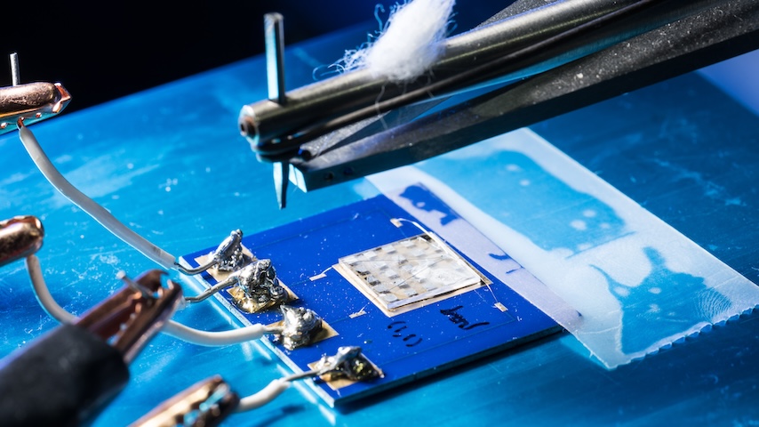
However, a major challenge is being able to diagnose these nanoscale thermal management challenges within electronic devices. To address that, Pickel’s team—comprised of two graduate and two Ph.D. students—has developed a noninvasive optical thermometry technique to map heat transfer using luminescent nanoparticles.
“Being able to get a really detailed temperature map on the nanoscale level would give a lot of really relevant information about what exactly is going wrong,” Pickel said.
Drawing inspiration
Although optical thermometry methods are popular, given that they’re based on light and are non-invasive, they can only reach a fundamental limit in spatial resolution of hundreds of nanometers at best. That’s not close enough to identify nanoscale components.
“For me, as someone who's worked on optical thermometry methods for a while, it's kind of like the Holy Grail, to be able to use an optical technique but get below that diffraction limit,” Pickel said.
 University of Rochester assistant professor Andrea Pickel (right) with materials science Ph.D. students Benjamin Harrington (left) and Ziyang Ye (center) in their lab in Hopeman Hall July 10, 2024. Photo: J. Adam Fenster/University of Rochester
“It was kind of in the back of my mind for many years, could you do this for thermometry?” Pickel recalled. “A couple of years before I started my own research group, there were some really cool innovations in the specific class of materials that my group does a lot of work with, which are upconverting nanoparticles [UCNPs]. Basically, people showed that you could do these kinds of super resolution techniques with those materials. That's what really inspired me to start thinking, okay, now that people have shown that, maybe we could think about doing this seriously for thermometry.”
How it works
While the biological imaging technique provided great inspiration, applying that method to electronics presented significant hurdles since the materials are so different.
“We use objective lenses like you’ve probably seen on a microscope. But for biology, often they'll have a liquid between the objective and the sample. That’s helpful from like an optical perspective in terms of improving your spatial resolution and signal to noise and stuff like that,” Pickel said.
But liquids and electronics obviously don't mix. And with the distance being so small between the sample and lens, there could be disruptions to the device or even changes to the temperature profile to be measured.
Instead, by applying highly doped UCNPs to the surface of a device, the researchers were able to achieve super high-resolution thermometry at the nanoscale level from up to 10 millimeters away. Highly doped UCNPs can convert near-infrared light into visible and ultraviolet light, making them luminescent.
Discover the Benefits of ASME Membership
In that 10-millimeter gap between the objective and the sample is simply air, but “now we can get spatial resolution that’s much, much higher. We estimate down to about 120 nanometers from our experiments,” Pickel said.
The team’s findings are detailed in, “Optical super-resolution nanothermometry via stimulated emission depletion imaging of upconverting nanoparticles.” In that work, Pickel’s team used an electrical heater structure that they designed to produce sharp temperature gradients.
“We definitely built on advances that others made in some of these UCNPs and showing that you could do the super resolution imaging,” she explained. “But then to do thermometry, we had to build new instrumentation. We’re not just doing imaging, of course, but we need to look at some kind of temperature dependent signal and so we do what’s called spectroscopy. We look at a much more detailed level like, what does the light being emitted by these nanoparticles look like? How does that change with temperature? How can we convert the emissions spectra that we record into temperature information?”
Next steps
The team hopes this method will eventually be a way to help manufacturers improve components for electronic devices. Two challenges still need to be further resolved before this technique can become more practical and broadly applicable.
First is the ability to place nanoparticles on the top of samples to be measured. “We developed some strategies for doing that, but there’s definitely room and a need to do more there. We need better control of how we place these particles onto the samples and that’s super key for practical applications,” Pickel said.
You Might Also Enjoy: Heat Transistor May Make for Cooler Computers
The second challenge circles around lasers, which are key to this method. Using UCNPs allows for the use of lower laser powers compared to other materials used to do similar kinds of imaging, but they are still “quite high,” she added. “The problem is that with high laser powers is, in some cases you can end up heating the samples where you're trying to measure the temperature. So, we’re trying to figure out how can we do this with even lower laser powers to try and avoid those issues.”
While electronic devices are the primary target at the moment, the technique could someday be used in other applications, such as helping with heat transfer issues in optoelectronic devices (LEDs or high-power laser diodes) or even determining the thermal properties of certain materials.
“We relied a lot on some more recent innovations—new compositions of these UCNPs to give them new capabilities. And then we borrowed self-assembly ideas that people have used for other reasons. Then we combined that with kind of our own heat transfer and thermometry knowledge,” Pickel said. “It’s been kind of interesting for me to see how we’ve kind of brought together so many different pieces. I think it’s been exciting to build on a lot of really cool accomplishments and great work that other people have done, but also show how, by bringing all these different pieces together, we could do something totally new and different.”
Louise Poirier is senior editor.
Taking inspiration from biological imaging, researchers have unlocked a new technique to identify overheated electronic components.

Managing editor, Mechanical Engineering magazine
Related Content


