3D Printing at Nano Scale Optimizes Quantum Sensing
3D Printing at Nano Scale Optimizes Quantum Sensing
Researchers develop a new way to fabricate complex crystalline structure for quantum sensors.
Sensors are widely used to measure and monitor parameters of all types across industries. Demand for more complex sensors has increased as they have become quite useful in an increasingly connected world. Quantum sensors help measure, navigate, and interact with environments at the atomic level.
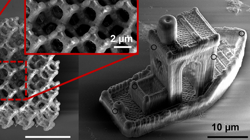
Researchers at the University of California, Berkeley's Laser Thermal Lab have developed a method of printing a tiny crystalline structure as the substrate for quantum sensors by mixing tiny, nanoscale diamonds into their resins as part of the 3D printing process. The team's test model structure, nicknamed “3DBenchy,” resembles a tugboat (shown above).
“We fabricate 3D printed structures at the microscale that have diamonds embedded inside of them,” explained Brian Blankenship, a doctoral candidate in mechanical engineering at the UC Berkeley's Laser Thermal Lab and a researcher on the team that developed the 3D printed structure. “We utilize nitrogen vacancy [NV] centers inside of diamonds as sensors. These are individual defects inside an otherwise crystalline diamond that have quantum properties.”
Although NV centers have been studied in the past and have shown favorable properties, the novelty of the Berkeley team’s work has been its ability to generate diamonds as 3D structures that can be given advanced geometries to suit the needs of different sensors, he continued.
You Might Also Enjoy: Graphene-based Biosensor Offers Instant Diagnosis
“For instance, we want to print filters and other microdevices inside of microfluidic channels so that we can measure different things inside of them such as the temperature, magnetic field, or the presence of different types of ions,” he said.
The lab utilizes a technique called two photon polymerization (TPP) to create microscale structures that have nanoscale feature sizes, Blankenship added.
 Nitrogen vacancy (NV) centers embedded in microscale structures with complex geometries. These structures use optical imaging to measure temperature and magnetic field inside of them. Photo: Brian Blankenship, UC Berkeley Laser Thermal Lab
“It’s an additive manufacturing technique that gives us even more design flexibilities than what is possible with many other more conventional additive manufacturing techniques, and it can print really small things,” he said.
Nitrogen vacancy (NV) centers embedded in microscale structures with complex geometries. These structures use optical imaging to measure temperature and magnetic field inside of them. Photo: Brian Blankenship, UC Berkeley Laser Thermal Lab
“It’s an additive manufacturing technique that gives us even more design flexibilities than what is possible with many other more conventional additive manufacturing techniques, and it can print really small things,” he said.
Much of the work in the team’s lab has focused on using this technique to create metamaterials, which are materials that have enhanced or unique properties relative to their bulk material counterparts due to their hierarchical architecture, Blankenship said.
“However, we wanted to measure what was going on inside of these materials and as they interact to external stimuli, which prompted us to explore these techniques,” he continued. “In the context of our paper, this additive manufacturing technique allows us to fix these quantum sensing particles into place, so that we can reliably measure different observables at those points.”
Become a Member: How to Join ASME
Quantum sensing is a new phase for a field that has been around for a while and used in many different applications, said Costas Grigoropoulos, a professor of mechanical engineering at UC Berkeley's Laser Thermal Lab and a member of the research team. For example, they are widely used in developing GPS technology as well as other applications.
“They come in a ton of varieties and forms. In our case, we leverage the quantum properties associated with the spin-states of the NV centers to detect and measure external fields and influences with high sensitivity and precision,” Grigoropoulos said. “Often, these sensors are implanted into relatively flat, crystalline substrates that are difficult to arrange in more complex ways. It’s especially difficult to vary the locations of these NV centers in three dimensions this way. We feel that our technique will open new possibilities for different applications because it gives us more design freedoms on what we can make that have these sensing abilities.”
This ability to create tiny crystalline structures was not possible using existing methods, but has the potential to boost the performance and capacity of optical sensors. The team believes that once the technology is refined, it will open new doors for science and technology.
Jim Romeo is an independent writer in Chesapeake, Va.
Researchers at the University of California, Berkeley's Laser Thermal Lab have developed a method of printing a tiny crystalline structure as the substrate for quantum sensors by mixing tiny, nanoscale diamonds into their resins as part of the 3D printing process. The team's test model structure, nicknamed “3DBenchy,” resembles a tugboat (shown above).
“We fabricate 3D printed structures at the microscale that have diamonds embedded inside of them,” explained Brian Blankenship, a doctoral candidate in mechanical engineering at the UC Berkeley's Laser Thermal Lab and a researcher on the team that developed the 3D printed structure. “We utilize nitrogen vacancy [NV] centers inside of diamonds as sensors. These are individual defects inside an otherwise crystalline diamond that have quantum properties.”
Although NV centers have been studied in the past and have shown favorable properties, the novelty of the Berkeley team’s work has been its ability to generate diamonds as 3D structures that can be given advanced geometries to suit the needs of different sensors, he continued.
You Might Also Enjoy: Graphene-based Biosensor Offers Instant Diagnosis
“For instance, we want to print filters and other microdevices inside of microfluidic channels so that we can measure different things inside of them such as the temperature, magnetic field, or the presence of different types of ions,” he said.
The lab utilizes a technique called two photon polymerization (TPP) to create microscale structures that have nanoscale feature sizes, Blankenship added.
Nitrogen vacancy (NV) centers embedded in microscale structures with complex geometries. These structures use optical imaging to measure temperature and magnetic field inside of them. Photo: Brian Blankenship, UC Berkeley Laser Thermal Lab
Much of the work in the team’s lab has focused on using this technique to create metamaterials, which are materials that have enhanced or unique properties relative to their bulk material counterparts due to their hierarchical architecture, Blankenship said.
“However, we wanted to measure what was going on inside of these materials and as they interact to external stimuli, which prompted us to explore these techniques,” he continued. “In the context of our paper, this additive manufacturing technique allows us to fix these quantum sensing particles into place, so that we can reliably measure different observables at those points.”
Become a Member: How to Join ASME
Quantum sensing is a new phase for a field that has been around for a while and used in many different applications, said Costas Grigoropoulos, a professor of mechanical engineering at UC Berkeley's Laser Thermal Lab and a member of the research team. For example, they are widely used in developing GPS technology as well as other applications.
“They come in a ton of varieties and forms. In our case, we leverage the quantum properties associated with the spin-states of the NV centers to detect and measure external fields and influences with high sensitivity and precision,” Grigoropoulos said. “Often, these sensors are implanted into relatively flat, crystalline substrates that are difficult to arrange in more complex ways. It’s especially difficult to vary the locations of these NV centers in three dimensions this way. We feel that our technique will open new possibilities for different applications because it gives us more design freedoms on what we can make that have these sensing abilities.”
This ability to create tiny crystalline structures was not possible using existing methods, but has the potential to boost the performance and capacity of optical sensors. The team believes that once the technology is refined, it will open new doors for science and technology.
Jim Romeo is an independent writer in Chesapeake, Va.
Related Content

Podcast: Inside the Engineering of a Czinger Hypercar
Mar 10, 2025
Chief engineer of Czinger Vehicles offers a look into the 3D printing technology shaping the future.
Mechanical Engineering Career Trends for Manufacturing
Feb 12, 2025

Breaking Barriers with High-Velocity Cold Bonding
Feb 3, 2025
High-speed metallic collisions can form strong, durable atomic bonds, which could unlock ways to enhance 3D printing and other manufacturing techniques.
Researchers to Create a Digital Library for Aircraft Parts
Sep 30, 2024
Some airframes are many decades old. Scanning and digitizing components could enable small manufacturers to produce replacement parts.